Dupa plasarea solicitării de comandă, in sectiunea Istoric puteti vedea cate solicitări de comandă mai avem de procesat inaintea dumneavoastra
Program de lucru: Luni - Vineri 9:00 - 18:00, pauza 13:00 - 14:00.
Se efectueaza lucrari de mentenanta la site si pot aparea erori. In cazul in care intampinati erori va rugam sa reincercati mai tarziu.
Ridicarea personala este disponibila pentru comenzile achitate in avans. Se pot ridica dupa ce sunt pregatite.
No products
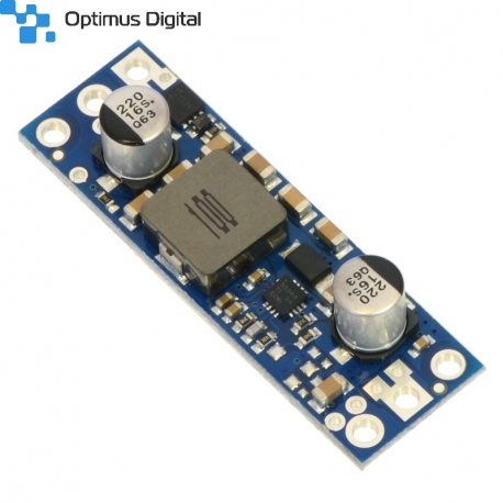 View larger
Pololu 6V Step-Up Voltage Regulator U3V50F6
0104110000037381
New product
This powerful boost regulator efficiently generates an output voltage of 6 V from an input voltage as low as 2.9 V while allowing an input current as high as 5 A.
See description for more details about the product.
Add to cart now!
This product is no longer in stock
- Write a review
- Remove this product from my favorite's list.
- Add this product to my list of favorites.
More info
Overview
These boost (step-up) voltage regulators generate higher output voltages from input voltages as low as 2.9 V. They are switching regulators (also called switched-mode power supplies (SMPS) or DC-to-DC converters) and have a typical efficiency between 80% to 95%. The available output current is a function of the input voltage, output voltage, and efficiency (see the Typical Efficiency and Output Current section below), but the input current can typically be as high as 5 A.
The U3V50x regulator family also includes two adjustable-output versions: the U3V50ALV offers an output range of 4 V to 12 V and the U3V50AHV offers an output range of 9 V to 30 V. The different versions of the board all look very similar, so the bottom silkscreen includes a blank space where you can add your own distinguishing marks or labels.

The no-load quiescent current will typically be between 1 mA and 5 mA for most combinations of input and output voltages, though the combination of a very high output voltage and a very low input voltage (e.g. when boosting from 3 V in to 30 V out) can result in quiescent currents on the order of a few dozen milliamps. The ENABLE pin can be used to put the board in a low-power state that reduces the quiescent current to approximately 20 µA per volt on VIN.
This regulator has built-in reverse-voltage protection, over-current protection, thermal shutdown (which typically activates at 165°C), and an under-voltage lockout that causes the regulator to turn off when the input voltage is below 2.5 V (typical).
Features
• Input voltage: 2.9 V to VOUT
• Fixed 5 V, 6 V, 9 V, 12 V or 24 V output with 4% accuracy
• 5 A switch allows for input currents up to 5 A
• Integrated reverse-voltage protection, over-current protection, over-temperature shutoff, and under-voltage lockout
• Typical efficiency of 80% to 95%, depending on input voltage, output voltage, and load
• Compact size: 1.9" x 0.6" x 0.41" (48 x 15 x 10.5 mm)
• Two mounting holes for #2 or M2 screws
• Smaller holes for 0.1" header pins and larger holes for terminal blocks offer several options for connecting to the board
Using the regulator
Connections
This boost regulator has four connections: input voltage (VIN), ground (GND), and output voltage (VOUT), and ENABLE.

The input voltage, VIN, must be at least 2.9 V and should not exceed the output voltage, VOUT. (If VIN is higher than VOUT, the higher input voltage will show up on the output, which is potentially dangerous for your connected load and could also damage the regulator.)
The regulator is enabled by default: a 100 kΩ pull-up resistor on the board connects the ENABLE pin to reverse-protected VIN. The ENABLE pin can be driven low (under 0.7 V) to put the board into a low-power state. The quiescent current draw in this sleep mode is dominated by the current in the pull-up resistor from ENABLE to VIN and by the reverse-voltage protection circuit, which will draw between 10 µA and 20 µA per volt on VIN when ENABLE is held low. If you do not need this feature, you should leave the ENABLE pin disconnected. Note that like most boost regulators, the input power will pass through to the output when the board is disabled, so the ENABLE pin cannot be used to turn off power to the load.
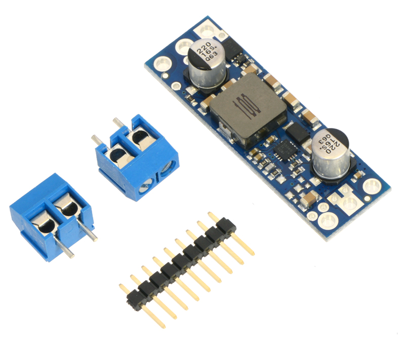
Pololu fixed step-up voltage regulator U3V50Fx with included optional terminal blocks and header pins.
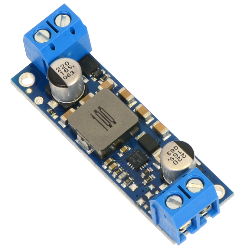
Pololu fixed step-up voltage regulator U3V50Fx, assembled with included terminal blocks.
The connections are labeled on the back side of the PCB, and the board offers several options for making electrical connections. The eight smaller through-holes on the ends of the board are arranged with a 0.1" spacing for compatibility with solderless breadboards, connectors, and other prototyping arrangements that use a 0.1" grid; you can solder pieces of the 9x1 straight male header strip into these smaller holes. Alternatively, you can solder the 2-pin 5mm-pitch terminal blocks to the two pairs of larger holes on the ends of the board. For the most compact installation, you can solder wires directly to the board.
Note that this regulator has a thick PCB (0.093"), so terminal block and header pins will not protrude as far through the holes as they would with typical 0.062"-thick PCBs.

Pololu step-up voltage regulator U3V50x with included terminal blocks installed, side view.
The board has two mounting holes intended for #2 or M2 screws. The mounting holes are at opposite corners of the board, separated by 1.7" horizontally and 0.4" vertically.
Typical efficiency and output current
The efficiency of a voltage regulator, defined as (Power out)/(Power in), is an important measure of its performance, especially when battery life or heat are concerns. As shown in the graphs below, these switching regulators have an efficiency of 80% to 95% for most combinations of input voltage, output voltage, and load.
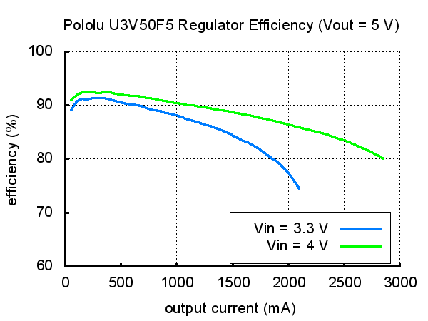
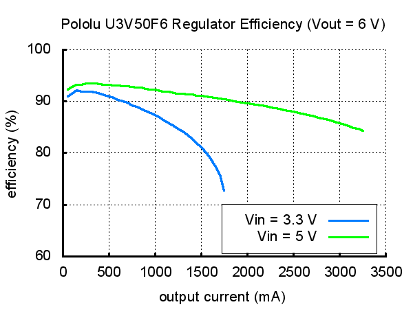
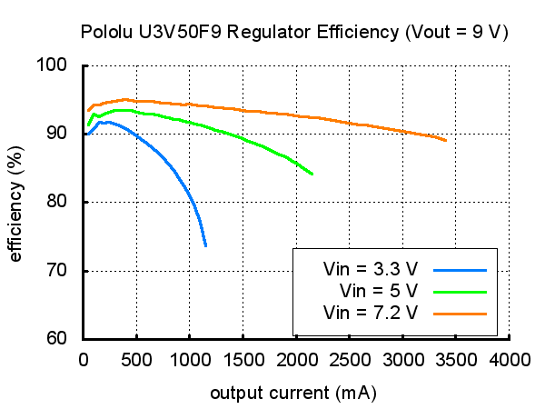
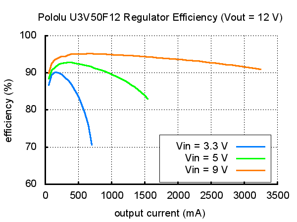
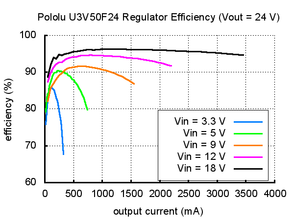
The maximum achievable output current is approximately proportional to the ratio of the input voltage to the output voltage. If the input current exceeds the 5 A switch current limit, the output voltage will begin to drop. Additionally, the maximum output current can depend on other factors, including the ambient temperature, air flow, and heat sinking.
During normal operation, this product can get hot enough to burn you. Take care when handling this product or other components connected to it.
Specifications
Dimensions
| Size: | 0.6" x 1.9" x 0.41"1 |
| Weight: | 7.5 g2 |
General specifications
| Minimum operating voltage: | 2.9 V |
| Maximum operating voltage: | 6 V |
| Maximum input current: | 5 A |
| Output voltage: | 6 V |
| Reverse voltage protection?: | Y |
| Maximum quiescent current: | 4 mA3 |
Notes:
1 Without included optional headers or terminal blocks. Height with terminal blocks installed is approximately 0.5".
2 Without included optional headers or terminal blocks. Terminal blocks add 3.4 g.
3 Typical worst case (i.e. with VIN at 3 V). Quiescent current depends on the input and output voltages and is much lower for most of the input voltage range. The ENABLE pin can be used to reduce the quiescent current to well under 1 mA.
Don't delay, buy today.
Add to cart now!
Reviews
Customers who bought this product also bought:
-
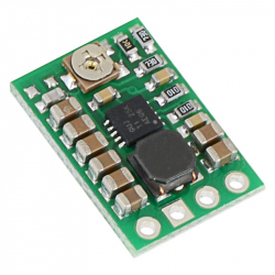
Pololu...
The S7V8A switching step-up/step-down regulator...
$16.80
-
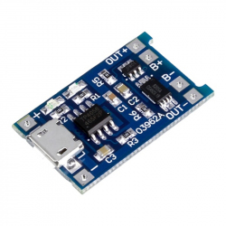
TP4056 Micro...
This is a micro USB Li Po battery charger...
$1.44
-
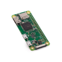
Raspberry Pi...
Raspberry Pi Zero W - one of the most powerful...
$12.97
-
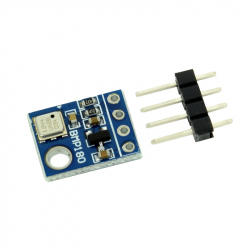
BMP180...
BMP180 sensor module is ideal for measuring...
$1.68
-

Raspberry Pi...
The 7" Touchscreen Monitor for Raspberry Pi...
$83.76
-
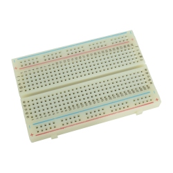
400p HQ...
This 400 pin board is constructed of...
$1.09
-
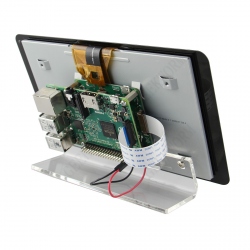
Plastic...
Plastic Stand for Raspberry Pi LCD See...
$4.80
-
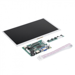
7'' LCD for...
Product size: 90.5 mm*65.6 mm*8 mm See...
$59.76
-
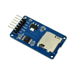
MicroSD Card...
This small SD card slot breakout board allows...
$1.05
-
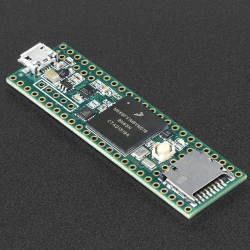
Teensy 3.6
Version 3.6 of the superb Teensy range features...
$52.56


